請致電:+86 0518-87284110
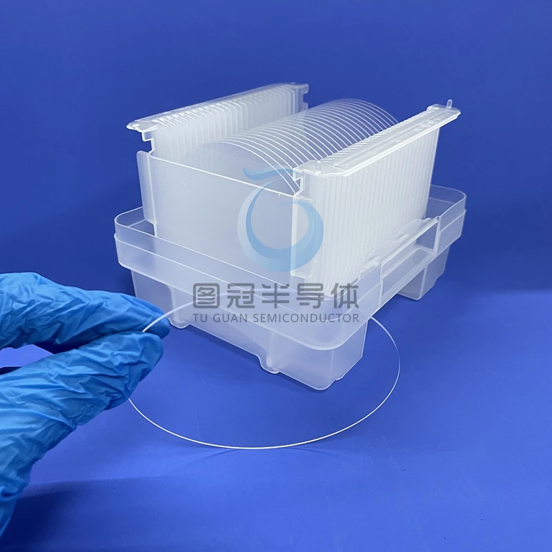
4 inch Quartz Wafers & Optical Substrates
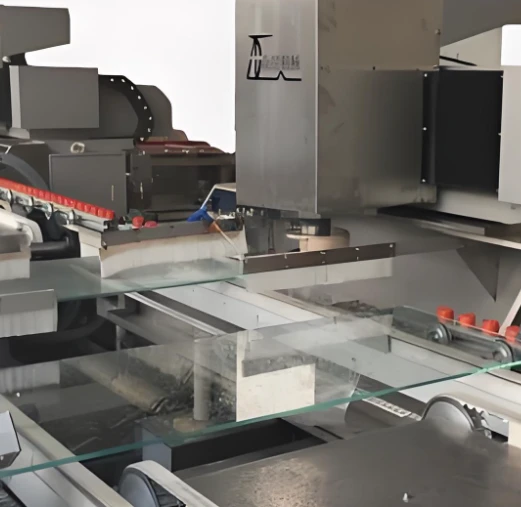
Our high-purity Fused Quartz wafers and optical substrates are engineered for demanding applications in semiconductor manufacturing, optical systems, and MEMS devices. Offering exceptional UV transparency, low thermal expansion, and superior surface quality, these wafers ensure precise, contamination-free performance in critical processing, testing, and lithography environments.
材料
- 基材:高純度合成熔融石英(SiO₂ ≥99.99%)
- 光學級: 低羥基(OH)含量的 UV 等級透明度
尺寸
- 直徑 :100 mm ±0.05 mm
- 厚度:3 mm ±0.05 mm
- 邊緣處理:細研磨的倒角 ≤0.3 mm
物理性質
- 密度: 2.2 g/cm³
- 硬度:Mohs 5.5-6.5
- 熱膨脹: 0.55 × 10⁻⁶/°C (20-300°C)
- 軟化點: 1683°C
光學性質
- 透射範圍:190 nm (UV) 至 2500 nm (IR)
- 折射率: 1.458 @ 587.6 nm (nd)
- Scratch-Dig: 60/40 (MIL-PRF-13830B)
- 表面平坦度: λ/4 @ 632.8 nm
表面規格
- Ra 粗糙度: ≤5 Å (拋光表面)
- 平行度 : ≤1 arcmin
化學耐性
- 耐酸(HF除外)、水和有機溶劑
應用
- 光學窗口,雷射系統,UV 光刻
- 半導體加工,高溫視窗
認證與符合性
- 符合 RoHS
- 可按需提供自訂量測報告
封裝
- 單獨包裝於防靜電泡棉中
- 裝於剛性、耐壓容器中運送
備註
避免機械衝擊或直接接觸鋒利物體
使用 IPA 或丙酮,並以無塵布巾清潔
如需完整技術資料或客製化需求,請聯繫 email