Call us: +86 0518-87284110
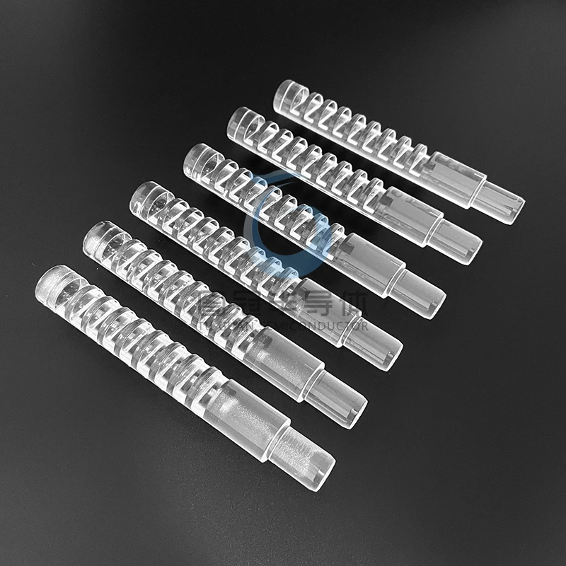
Fused Quartz Wafer Spacers & Stacking Rods
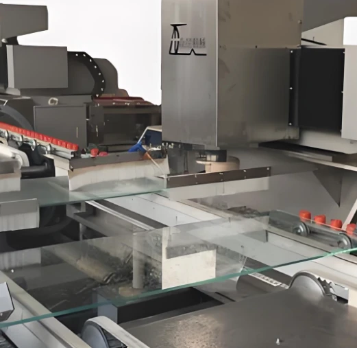
Fused quartz wafer spacers and stacking rods designed for wafer separation, drying, and batch handling in wet benches, diffusion furnaces, and high-temperature processes. Made from high-purity fused silica and finished for low particle generation, these components keep wafers evenly spaced, prevent scratching, and deliver clean, thermally stable performance in critical environments.
What to Provide for a Quote
- Drawing (PDF/STEP) or key dimensions: rod/bar diameter or width × length; groove/serration pitch, width, and depth; contact land width
- Wafer size and target spacing (number of wafers per rod, total stack height)
- End features: reduced-diameter tenon/shoulder, flat/anti-roll surfaces, cross-holes, threads, or mounting slots
- Surface finish on contact areas (polished vs. ground), edge radii/chamfers to protect wafer edges
- Operating environment: chemicals (wet bench chemistries), vacuum/temperature profile, cleanliness level
- Critical tolerances: groove pitch uniformity, straightness/concentricity, allowable deflection under load
- Quantity (prototype or batch), required inspection reports, packaging level
Key Specifications
- Material: High-purity fused quartz (SiO₂); material certificate available by request
- Geometry: Round rods or flat bars with machined grooves/serrations; optional standoffs, stops, or alignment flats; single-piece or flame-fused assemblies
- Dimensions: Per drawing (made-to-order) with uniform section thickness for thermal stability
- Contact Surfaces: Polished lands and radiused edges to minimize micro-chipping and scratches
- End & Mounting Options: Tenons/shoulders for frames, threaded or through-hole ends, anti-rotation flats, laser part ID by request
- Cleanliness: Ultrasonic/DI cleaning; Class-100 compatible packaging
Material Properties (Typical)
- Very low thermal expansion and good thermal-shock tolerance
- Excellent chemical resistance to most process media (note: HF attacks quartz)
- Electrically insulating, low outgassing; optically clean surfaces
Processing & Design Notes
- Match groove radius and land width to wafer edge geometry; avoid sharp transitions
- Keep groove pitch uniform to ensure consistent spacing and airflow/rinse flow; add drainage reliefs where needed
- Specify allowable deflection under full load; use larger section or ribs if stiffness is critical
- Vent any blind holes used in vacuumed tools to prevent virtual leaks
- Stress-relief annealing and edge polishing recommended for long life in thermal cycling
Inspection & Testing
- Dimensional verification: rod diameter/length, groove pitch/width/depth, end-feature sizes and positions
- Straightness/concentricity checks and deflection under representative load
- 100% visual inspection for chips, micro-cracks, inclusions, and contamination
- Optional: cleanliness certification, birefringence/stress evaluation
Applications
Wafer stacking and separation in wet benches, diffusion/oxidation/bake furnaces, drying and transport fixtures, temporary storage racks, and precision handling in high-purity lines
Packaging & Storage
Contact-surface protectors and separators; anti-static, vacuum-sealed packaging with rigid outer protection. Store dry (<40% RH) at 10–30 °C and away from HF-containing chemicals.
Notes
Custom configurations (hole patterns, coatings, or additional markings) available upon request.
Compliance certificates (RoHS, ISO 9001) provided with bulk orders.