Call us: +86 0518-87284110
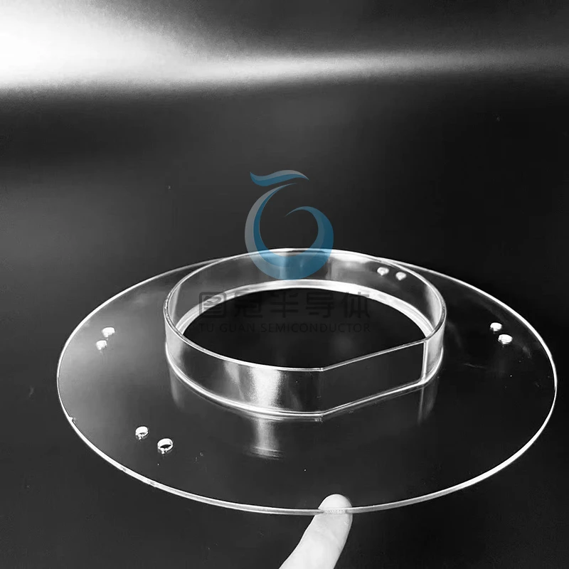
Fused Quartz Focusing & Plasma Rings for Etch and CVD
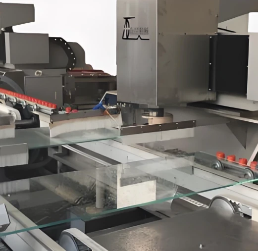
Custom fused quartz focusing rings (also called edge rings, confinement rings, plasma rings, or shadow rings) engineered for plasma etching, CVD, and other vacuum processes. Made from high-purity fused silica and precision-machined to your drawing, these rings deliver excellent plasma resistance, thermal stability, and tight dimensional control—helping maintain process uniformity and minimize contamination inside critical chambers.
What to Provide for a Quote
- Drawing (PDF/STEP) or key dimensions: outer diameter, inner diameter, thickness, step heights/widths
- Wafer size and orientation (e.g., 200/300 mm; notch position), target ring-to-wafer gap
- Features: steps/ledges, pockets, clamp or shadow geometry, vents, bolt holes, countersinks, alignment notches
- Edge details and surface finish (chamfer/bevel; ground or polished surfaces)
- Operating conditions: plasma chemistry, power, temperature, expected lifetime/erosion allowance
- Critical tolerances: flatness, parallelism, concentricity, runout
- Quantity (prototype or batch), required inspection reports, packaging level
Key Specifications
- Material: High-purity fused quartz (SiO₂); material certificate available by request
- Geometry: Flat rings, stepped/ledged rings, multi-piece segments, confinement/shadow rings—fully custom per drawing
- Dimensions: Per drawing (made-to-order); uniform section thickness for thermal stability
- Functional Features: Shadow lips, clamp lands, wafer seating steps, flow/vent holes for pressure equalization
- Edge & Surface: Fire-polished rims; ground or polished functional surfaces; smooth radii to reduce particle generation
- Alignment & Mounting: Notches/keys, countersunk holes, datum references, laser part ID/flow direction by request
- Cleanliness: Ultrasonic/DI cleaning; Class-100 compatible packaging
Material Properties (Typical)
- Low thermal expansion and high thermal-shock resistance
- Excellent chemical inertness to most process gases; note that HF attacks quartz
- Electrically insulating, low outgassing; optically clean surfaces
Processing & Design Notes
- Keep ring-to-wafer gap and step heights consistent to ensure uniform plasma distribution
- Add generous internal radii at transitions to reduce stress and particle traps
- Vent/counterbore through-holes that see vacuum to prevent virtual leaks
- Select surface finish based on process cleanliness and clamp/shadow requirements
- We can advise feasible tolerances for flatness, parallelism, concentricity, and runout based on size/geometry
Inspection & Testing
- Dimensional verification (CMM/optical): OD/ID/thickness, step heights/widths, gap features
- Flatness/parallelism and runout checks against datum surfaces
- Visual inspection: 100% check for chips, micro-cracks, inclusions, and contamination
- Optional: birefringence/stress evaluation; surface finish verification; cleanliness report
Applications
ICP/RIE/DRIE plasma etching, PECVD/CVD, as edge/focusing/shadow rings and confinement components for 150–300 mm wafer platforms and custom substrates
Packaging & Storage
Anti-static, vacuum-sealed packaging with rigid protection; ring separators to prevent edge contact. Store dry (<40% RH) at 10–30 °C; keep away from HF-containing chemicals.
Notes
Custom configurations (hole patterns, coatings, or additional markings) available upon request.
Compliance certificates (RoHS, ISO 9001) provided with bulk orders.