お電話ください:+86 0518-87284110
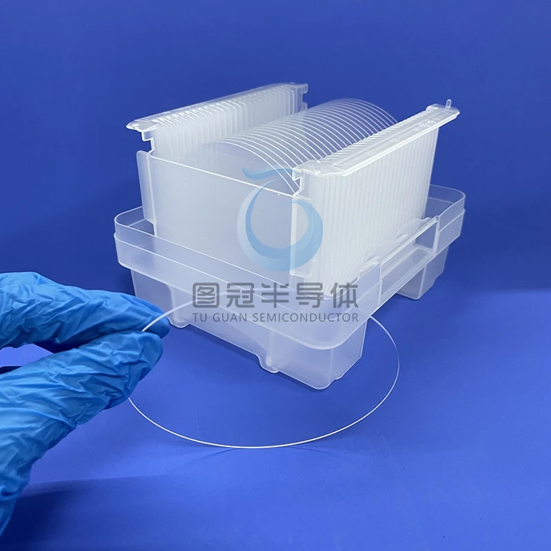
4 inch Quartz Wafers & Optical Substrates
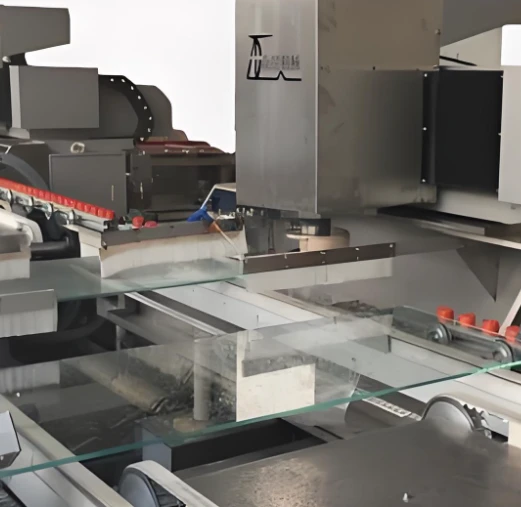
Our high-purity Fused Quartz wafers and optical substrates are engineered for demanding applications in semiconductor manufacturing, optical systems, and MEMS devices. Offering exceptional UV transparency, low thermal expansion, and superior surface quality, these wafers ensure precise, contamination-free performance in critical processing, testing, and lithography environments.
材質
- ベース材料:高純度合成溶融石英(SiO₂ ≥99.99%)
- 光学グレード: OH含有量が少ないUVグレードの透明性
寸法
- 直径 :100 mm ±0.05 mm
- 厚さ: 3 mm ±0.05 mm
- エッジ処理: 細研磨の面取り ≤0.3 mm
物理的性質
- 密度: 2.2 g/cm³
- 硬度: Mohs 5.5-6.5
- 熱膨張: 0.55 × 10⁻⁶/°C (20-300°C)
- 軟化点: 1683°C
光学特性
- 透過範囲:190 nm (UV) から 2500 nm (IR)
- 屈折率: 1.458 @ 587.6 nm (nd)
- Scratch-Dig: 60/40 (MIL-PRF-13830B)
- 表面の平坦度: λ/4 @ 632.8 nm
表面仕様
- Ra 粗さ: ≤5 Å (研磨表面)
- 並列度 : ≤1 arcmin
化学的耐性
- HFを除く酸・水・有機溶媒に耐性がある
用途
- 光学窓、レーザーシステム、UVリソグラフィ
- 半導體加工、高温用ビューポート
認証と適合
- RoHS適合
- カスタム計測レポートはご要望に応じて提供可能
パッケージング
- 個別に静電防止フォームで包装されています
- 頑丈で粉砕耐性のある容器で出荷
備考
機械的な衝撃を避け、鋭利な物体との直接接触を避けてください
IPAまたはアセトンを使い、糸くずの出ないウェスで清浄にしてください
完全な技術データまたはカスタムリクエストについては、emailまでご連絡ください